COMMON SOURCE AMPLIFIER
Common-source amps: Versatile workhorses for voltage amplification.
0
105
Common Source Amplifier
- If you connect the input signal to the gate terminal and the source terminal, the output voltage is increased and found across the resistor at the load in the drain terminal.
- An amplifier with a shared source is what this is. The source in this case connects the input and output together. It's also called a transconductance amplifier or a voltage amplifier.
- According to the input impedance and output impedance, it produces current gain and voltage gain.
- In these circuits, FETs are used to bring about voltage gain and high input resistance.
Circuit for a Common Source Amplifier

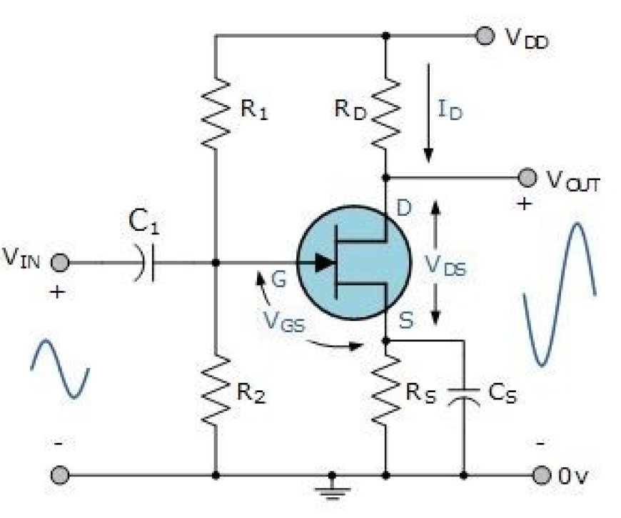
The following picture shows the circuit design of a typical source amplifier that has an N-channel FET and the ability to couple and bias.
- The common-emitter follower of a bipolar junction transistor will be like this circuit.
- The incoming signal will have the wrong polarity if we use a P-channel FET.
Common-Source Amplifier Circuit
Using a Common-Source Amplifier
- It is possible for this amplifier to work as both a voltage amplifier and a transconductance amplifier.
- If the amplifier is a transconductance amplifier, the signals that come in are boosted and change the amount of current that flows to the load.
- The input signal is amplified when the amplifier works as a voltage amplifier. As per Ohm's law, this alters the voltage across the load resistor and the current flowing through the FET.
- From the above circuit design, you can understand how the common source amplifier works. It works in the same way that a common-emitter follower of the BJT circuit does.
- It works when the signal from the input is sent to the gate port through capacitor C1.
- To determine whether any DC energy from the step before it has an impact on the gate terminal, use this capacitor.
- The potential is held by the 1Megaohm resistor R2 that is between the gate and the ground.
- The voltage is built up across the R2 resistor, which keeps the source above ground.
- The extra gain for the AC input comes from the bypass capacitor C2.
- The voltage that is increased comes from the load at the drain point of the circuit and the resistor R3.
- By stopping or getting rid of the DC parts, capacitor C3 connects this boosted output voltage to the AC signal of the next stage.
- This amplifier makes a signal that is 180 degrees out of phase with the signal that goes into it. This signal has a high power gain.
- The P-channel common source amplifier using FET works the same way as the N-channel common source amplifier FET, but the voltage phases will be switched.
- There will be no current going between the gate and the source when the bias is reversed. So, there is no current in the gate.
- After that, the gate voltage (DC) is given as
Vg = Ig x Rg
Vs = Id x Rs gives you the DC voltage at the source.
Then, the source's voltage comes from the gate.
Formula: Vgs = Vg - Vs = 0-Id x Rs
Since Ig = 0,
Vgs = -Id x Rs
Where Id = drain current
Vgs = gate-source voltage
Vg = gate voltage
Rs = resistor at the source
Rg = resistor at Gate
Ig = gate current
- DC parts moving through the drain current can make the resistor Rs self-bias and feed back to the input from the output.
Applications
- Here are some ways that a standard source booster can be used.
- They are used to boost sensor signals, low-noise RF signals, communication systems like TV and FM antennas, as voltage-controlled parts in op-amps, and as cascade amplifiers and RF amplifier circuits.