BACKWARD DIODE
Backward Diodes: Tiny but Mighty! Detect Weak Signals, Act as High-Speed Switches (RF Mixers).
0
69
- A diode is a semiconductor part with two ends that is used in almost all electronic products. One can find tunnel, Schottky, zener, LED, PIN, backward, avalanche, laser, varactor, gunn,
- BARITT, and other kinds of diodes on the market. These are used depending on the need. In this case, the backward diode is a type of diode that works in reverse bias mode.
- This diode is like a tunnel diode or a Zener diode, but it works better with small reverse biases than with small forward bias voltages.
- This page gives some basic information about the backward diode, including how it is made, how it works, and what it can be used for.
Backward Diode
- A backward diode, also written "back diode," is a diode that works in reverse-biassed mode. It's a type of PN junction diode that's mostly made to give tunnel diodes and zener diodes different design features.
- This diode works in only one way, so it is called a solitary device. This diode works the same way as Zener and tunnel diodes, even though its working voltages are much lower
- Low-voltage messages between 0.1 volts and 0.6 volts are what the backward diode is for. This diode can also be used as a switch in the multiplier and RF mixer because it can switch quickly.
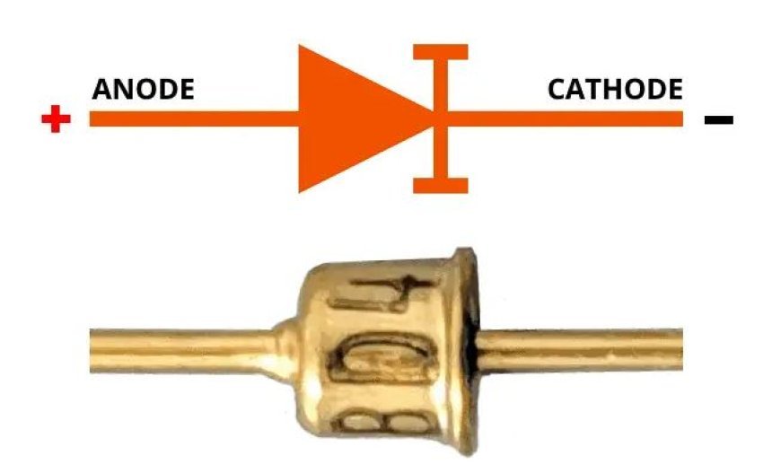
- Look at this picture of a backward diode that looks like a PN junction diode.
- On the other hand, the anode side (P-type) is the same as the PN junction, while the cathode side (N-type) is slightly different because of the bar.
Backward Diode SymbolBackward Diode Construction
- Aside from the light doping dosage, this diode is built like a tunnel diode.
- One side of the junction is lightly doped, while the other side is heavily doped.
- It helps line up the valance and conduction bands so that it works like a PN junction diode when the bias is applied forward.
- There is no tunnel current or quantum tunnelling when the bias is forward.
- But there is a huge tunnel current when the bias is backward. It is called a backward diode because it has better conduction and smaller resistance when quantum tunnelling only happens in reverse bias.
Working
- The quantum tunnelling concept is all that a backward diode does.
- Quantum tunnelling is a way to use quantum mechanics when wavefunctions can pass through a potential barrier. So the transfer through the potential barrier can be set and changes greatly with the height and width of the barrier.
- This diode works like a tunnel diode, except that the tunnelling happens when the bias is turned around.
- It works like a normal PN junction diode in both forward and reverse bias; in reverse bias, it can carry current better than in forward bias.
- A simple way to explain how this diode works is to look at an energy band diagram for different biases.
Backward Diode V-I Characteristics
- The backward diode's V-I features are shown below. This property demonstrates the main connection between the current and voltage in the device.
- The x-axis shows the voltage across the characteristic, and the y-axis shows the current flowing through it.
- The voltage-current (VI) features of a backward diode are different from those of other diodes.
- If you plot the current going through the diode against the voltage across it, you can see that the VI characteristics of a backward diode behave in a unique way, especially when it is operating in the reverse-biassed mode.
Forward-biassed region
- When the bias is on the forward side, the backward diode works like any other diode.
- The VI characteristics are very close to those of a normal diode, and it lets current run with very little resistance.
- The forward current through the diode grows exponentially as the forward voltage rises. This is the normal behaviour of the diode.
Reverse-biassed region
- In the reverse-biassed area, there is the biggest departure from the normal behaviour of a diode.
- The backward diode doesn't break down in an avalanche like other diodes do; instead, it has an area of negative resistance because of quantum tunnelling effects.
- The VI graph shows that as the reverse voltage goes up, the reverse current goes down in the negative resistance area.
- In normal diodes, the reverse current grows exponentially as the reverse voltage rises during avalanche breakdown. This is the opposite of what happens here.
- In a backward diode, the negative resistance area is the most important part of the VI properties.
- It lets the diode carry current when the bias is reversed, which is useful in some situations, especially when working with high-frequency oscillators, microwave generation, and parametric amplification.
Reverse breakdown region
- If you raise the reverse voltage above a certain point, the backward diode will finally reach a breakdown area where the reverse current rises very quickly.
- The negative resistance region is not the same as this region. This region is similar to how regular diodes behave when they go through avalanche breakdown.
- In the forward-biassed mode, a backward diode's VI characteristics behave like any other diode's. However, in the reverse-biassed mode, they show a unique area of negative resistance because of quantum tunnelling effects.
- Because of this, backward diodes are useful parts in certain situations where negative resistance and special electrical properties are needed.