SILICON CONTROLLED RECTIFIER
The Silicon Controlled Rectifier (SCR) is a three-terminal semiconductor device that acts like a switch for high power applications.
0
230
- The silicon controlled rectifier (SCR), which is also called the Thyristor, is a three-terminal, four-layer semiconductor device that controls current only in one way.
- It's mostly made of silicon materials and is used to handle a lot of power and change a lot of AC current into DC current. This is why it's referred to as a silicon-controlled rectifier.
- In the same way that the p-n junction diode does, the SCR lets electricity flow in one direction but not the other.
- There are two types of semiconductors in a standard p-n junction diode: p-type material and n-type material.
- On the other hand, an SCR is made up of four layers of semiconductors that switch between p-type and n-type materials.
- On SCR, there is a Gate terminal as well as an Anode and Cathode connector.
- Bell Laboratories' Tanenbaum, Goldey, Moll, and Holonyak came up with the idea of four-layer (P-N-P-N) switching in 1956.
- Gordon Hall led a team of power engineers who created the silicon-controlled rectifier (SCR), which Frank W. "Bill" Gutzwiller then sold.
- This is the brand name that General Electric uses for a certain type of Thyristor.
- Thyristors like TRIAC, SCS, DIAC, and others are used less often than SCR. This is why the device is often called a Thyristor.
- A lot of different things use SCRs, such as rectifying, controlling power, inverting, and more.
- It controls the amount of power that goes into the output terminal and is an important part of almost all current switching power sources.
Silicon Controlled Rectifier (SCR)
- There are three ends to a Silicon Controlled Rectifier (SCR): the Anode (A), the Cathode (K), and the Gate (G).
- The gate input or biasing state of the SCR can be changed to turn the device ON or OFF.
- The following picture shows the schematic sign for SCR. The way of normal current flow is shown by the diode's arrow.
Construction of a Silicon-Controlled Rectifier (SCR)

- An SCR is a four-layer, three-terminal semiconductor device at its core.
- It is made up of four layers of semiconductors that switch between p-type and n-type materials to make a PNPN or NPNP structure.
- Because of this, it has three p-n junctions, which are called J1, J2, and J3. Because of the way they are built, these joints may be alloyed or spread.
- In the PNPN structure, the three terminals are set up so that the Gate (G) terminal is closer to the Cathode (K) terminal and connected to the p-type layer. This is called the Anode (A) terminal. The picture below shows a standard SCR structure with P-N-P-N layers (PNPN form).
- Here, the anode (A) is an electrode that is positively charged, and this is where the normal current comes in.
- Cathode (K) is an electrode that is negatively charged, and this is where normal electricity leaves the gadget.
- The gate (G) controls the flow of electricity between the anode (A) and the cathode (K).
- In an SCR with a PNPN shape, the Anode (A) terminal is linked to the first P-type layer, and the Cathode (K) terminal is linked to the last N-type layer.
- As you can see in the picture above, the gate (G) contact is linked to the second p-type layer that is closer to the cathode (K).
- The first and last N-type layers, which are on the outside of SCR, have a lot of doping, but the middle P-type and N-type layers only have a little doping.
- When it comes to SCR, silicon is used to make the P-type and N-type layers because it has a very low leakage current compared to germanium.
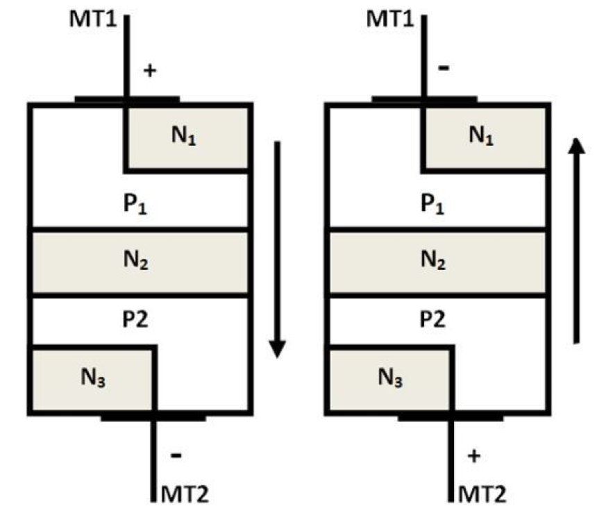
- One SCR is made up of one PNP transistor (Q1) and one NPN transistor (Q2). This can be seen from the shape of the SCR.
- The emitter of Q1 is the SCR's anode terminal, and the emitter of Q2 is the cap terminal. The collector of Q1 is linked to the base of Q2, and the base of Q2 is linked to the collector of Q1.
- Q2's base is linked to the Gate station of the SCR. The idea that SCR is like two transistors put together is known as the "two transistor model."
The Silicon Controlled Rectifier (SCR) can work in the following ways:
Modes of operation in a Silicon Controlled Rectifier (SCR)
- There are three ways that SCR can work, depending on how it is biased.
- The SCR's Anode (A) terminal is given a positive voltage (+) and the Cathode (K) terminal is given a negative voltage (-). This is the first method of action. It's possible for the Gate (G) port to be open.
- Forward Blocking Mode (Off State)

- It is at this point that junctions J1 and J3 are forward biased and junction J2 is backward biased.
- The current can't move from junction J1 to junction J3 because of the depletion area at junction J2. It acts as a wall between them. In spite of this, a small amount of escape current runs between J2 and J3.
- When the voltage across the SCR hits a certain point, the avalanche failure happens because of minority carriers with a lot of energy.
- At this breakdown voltage, the current starts to flow through the SCR. Below this voltage, there is no current flow because the SCR has a very high resistance to the current below the breakdown voltage and blocks the forward current as an open switch. As a result, it will be turned off.
- The SCR is in forward biasing mode, but there is no current flowing through it. This can be seen from above. The name of this mode of action comes from the fact that it locks forward.
2. Forward Conducting Mode (ON State)

- The SCR moves from blocking mode to conduction mode in this mode.
- One way is to raise the forward bias voltage (the voltage between the anode and cathode) above the breakdown voltage.
- The other is to apply a positive pulse or voltage at the gate point.
- In the first case, the forward bias voltage between the anode and cathode is raised above the breakdown voltage.
- This causes the depletion region to break down at J2, and current starts to flow through the SCR.
- The SCR will be in an ON state in this case. As you can see in the V-I Characteristics table below, the current flow in the SCR quickly rises after the connection breaks. This is the second case.
- A small positive pulse, or voltage VG, is sent to the SCR's Gate input, as seen in the picture above.
- The reversely biased junction J2 in forward blocking mode will become forward biased when the gate voltage is applied to the gate input. This makes the depletion region's width very small.
- In this case, a small forward bias voltage between the anode and the cathode can easily get through this small depletion area. So, when a small forward bias voltage is applied, an electric current flows through the SCR, turning it on.
- The gate voltage is no longer needed to keep the SCR in the ON state once it starts to conduct.
- Latching current is the smallest current that the SCR needs to stay ON after the gate voltage VG is taken away.
- If you use any of these ways, the avalanche breakdown happens at junction J2. This makes the SCR go into conduction mode, which makes it a closed switch that lets current run through it.
- In this case, the SCR is skewed forward, and electricity passes through it. It is for this reason that this mode of action is called forward-conducting mode.
3. Reverse Blocking Mode (OFF State)

- In this mode, the Cathode (K) terminal gets a positive voltage (+) and the Anode (A) terminal gets a negative voltage (-).
- The Gate (G) terminal is not connected to anything.
- There are three areas that make up the V-I traits of SCR.
These are them:
V-I Characteristics of Silicon Controlled Rectifier (SCR)

1. Forward Blocking Region
- The number OA in the V-I graph indicates the forward blocking area. This area shows how the SCR works in forward-blocking mode.
- The forward bias voltage is sent to the SCR in this area.
- The positive voltage goes to the anode, the negative voltage goes to the SCR, and the gate is open.
- When this happens, junctions J1 and J3 become forward biased, while junction J2 becomes backward biased.
- A small amount of current leaks from the SCR's anode terminal to its cathode terminal. This current is called a forward leakage current. In this area, the SCR is not conducting electricity, and the gadget is turned off.
2. Forward Conduction Region
- In terms of V-I properties, the area BC is known as the forward conduction region. This area shows the forward conduction state of the SCR's working.
- The current going from the anode to the cathode quickly rises in this area. As soon as the forward bias voltage between the anode and cathode goes above the breakdown voltage, the depletion region breaks down at junction J2. This lets current flow through the SCR, turning it on. After junction J2 breaks, the flow of current in this area speeds up very quickly.
- When the gate is open, the voltage at which the circuit breaks down is called the forward breakdown voltage (VBF).
- The area AB in V-I traits shows that the voltage across the SCR drops to a certain level as soon as it turns on.
3. Reverse Blocking Region
- In terms of the V-I traits, the region OE is known as the backward blocking region. This area shows the SCR's backward blocking mode of action.
- The reverse bias voltage is applied to the SCR in this area, where the Cathode is given a positive voltage, the Anode is given a negative voltage, and the Gate contact is left open.
- Junctions J1 and J3 are backward biased in this case, while the junction is forward biased.
- It is not possible for current to run through SCR because junctions J1 and J3 are reverse biased.
- However, there is a small leaky current flow in the SCR because the charge carrier moves in joint J2, which is forward-biased. This current flow is not enough to turn on the device. In this area, the SCR will be turned off because of this.
- An avalanche breakdown happens when the reverse bias voltage between the anode and cathode goes above the reverse breakdown voltage (VBR).
- At this point, the current rises very quickly. The area EF in V-I features is called the reverse avalanche region.