FET BIASING
FET biasing typically involves setting voltage levels to control the operation of a Field-Effect Transistor (FET).
0
55
FET BIASING
- It is the process of setting the starting working conditions (current and voltage) of an active device in an amplifier.
- A steady (DC) current or voltage at the ends of many electronic devices, like diodes, transistors, and vacuum tubes, is needed for them to work properly.
- These devices handle time-varying (AC) data. It is a bias that this current or voltage is. The AC information that is sent to them is placed on top of this DC bias current or voltage.
- For a transistor to work right, it needs to have the right polarity of external voltage applied across its emitter-base and collector-base joints. This is how transistors are biased.
- Thermal runaway doesn't happen with FETs like it does with BJTs. With a simple fixed-gate bias voltage, however, ID values are hard to predict because the highest and minimum transfer characteristics are so different.
- Source resistor and potential divider bias methods must be used to get acceptable limits on drain currents ID and voltages VDS and VDS between the drain and source.
- Most of the time, MOSFET bias circuits are the same as JFET bias circuits. We will talk about different FET biasing circuits used in designing, making, and putting together printed circuit boards (PCBs).
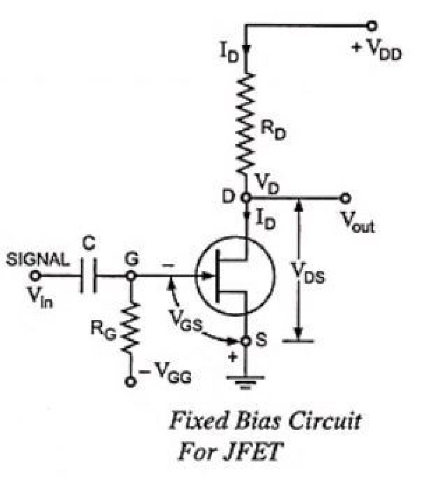
Fixed Bias

- To get the drain current ID you want from a FET device's DC bias, you have to set the gate-source voltage VGS.
- On a JFET, the saturation current IDS controls how much current can flow down the drain. The FET has a very high input resistance, so there is no gate current flow.
- The FET also doesn't change or load the DC voltage of the gate, which can be set by a voltage divider or a fixed battery voltage.
Fixed Bias Circuit
- A battery VQS is used to get a fixed DC bias. From the source, this battery makes sure that the gate is always negative and that there is no current flowing through the resistor RG and the gate wire, which means that IG = 0.
- The battery gives the N-channel JFET a voltage VGS to bias it, but no current is drawn from the battery VFF. It has a resistor RG that lets any AC signal that goes through capacitor C build up across RG.
- The DC voltage drop across RG is equal to IGRG, which is 0 volts. An AC signal will flow across RG.
- The voltage at the gate source (VGS) is then
- The equation for VGS is -VG – Vg = -VGG – 0 = -VGG.
- The equation then tells us that the gate-source voltage sets the drain-source current ID.
- After this current flows, there is a drop in voltage across the drain resistor RD. VRD = ID RD and the output voltage shows this drop.
Vout = VDD - IDRD
Self-Bias
Most of the time, this is how a JEFT is biased. The following picture shows a self-bias circuit for an N-channel JFET.
Self-bias circuit

- Due to the reversed bias, there is no gate current flowing through the gate source, so
IG = 0, and VG = iGRG =0.
- When there is a drain current ID, the voltage at the S is
VS = IDRS
- The voltage at the gate source is then
- The equation for VGS is VG minus VS = 0 minus IDRS = -IDRS.
- That is, voltage drops through resistance. The biasing voltage VGg comes from RS. There is no need for an outside source for biasing, which is why it is called "self-biasing."
- From the equations below, it's easy to find the working point, which is the point where signal ID and VDS are both zero.
- The formula for VDS is VDD - ID(RD + RS).
- So, the DC conditions of the JFET amplifier are now completely clear. A JEFT's self-biasing keeps its working point stable even if its properties, such as transconductance, change.
- If the given JFET is switched out for another one with double conductance, the drain current will also try to double.
- However, if the voltage drop across RS goes up, the gate-source voltage (VGS) goes down, which limits the increase in drain current.
Possible Divider Bias

- The circuit in the figure below gives us a slightly changed type of DC potential-divider bias. Between the drain source VDD and the resistors RG1 and RG2, there is a potential difference.
- The voltage V2 across RG2 offers the necessary bias. The extra gate resistor RG1 from the gate to the source voltage makes it easier to change the DS bias point and lets you use a bigger RS.
Bias Circuit for Potential Divider
The gate is biased backwards, so IG = 0 and gate voltage
VG = V2 = (VDD/R G1 + RG2)*RG2
And
The formula for VGS is VG-VS = VG-IDRS.
Because of how the circuit is set up, ID RS is bigger than VG, which means VGS is negative.
This gives you the right bias voltage.
You can find the working point by
ID = (V2 - VGS)/RS and
VDS = VDD - ID(RD + RS)